Cu-Mo/Cu-Ti Etching Solution in Incorporated Circuits
Etching solutions are crucial in the complex fabrication of integrated circuits (ICs), facilitating precise shaping and patterning of semiconductor materials. Notably, solutions containing Copper-Molybdenum (Cu-Mo) and Copper-Titanium (Cu-Ti) have emerged as focal points due to their distinct properties and relevance in IC production. This outline intends to examine Cu-Mo/Cu-Ti etching solutions comprehensively, covering aspects such as composition, preparation, application, benefits, limitations, and prospects within the IC sector.
Basics of Cu-Mo/Cu-Ti Etching Solution
Definition and Composition
The Cu-Mo/Cu-Ti Etching Solution is a specialized chemical solution utilized within the etching process for integrated circuits, advanced-generation displays (G8 and above), and flexible panels. Engineered for precision and adaptability, this solution is designed to selectively remove specific layers, such as copper (Cu), molybdenum (Mo), and titanium (Ti), within multilayer systems while preserving others. This selectivity is crucial for achieving intricate patterns necessary in the microfabrication of sophisticated electronic components.
Role in IC Fabrication Process
The Cu-Mo/Cu-Ti Etching Solution serves a vital role in the fabrication process of integrated circuits. It enables the precise removal of targeted layers, allowing for the creation of intricate circuit patterns and structures essential for the functionality of ICs. By selectively etching away specific materials while leaving others intact, this solution plays a key role in defining the circuitry and features of ICs, contributing to their performance and reliability.
Properties and Characteristics
Cu-Mo/Cu-Ti Etching Solutions exhibit several properties and characteristics that make them suitable for use in IC fabrication:
- Selectivity: These solutions have the ability to selectively remove specific materials while leaving others unaffected, enabling precise patterning and shaping of semiconductor layers.
- Chemical stability: They maintain stability and effectiveness over extended periods, ensuring consistent etching performance throughout the fabrication process.
- Compatibility: Cu-Mo/Cu-Ti Etching Solutions are compatible with a wide range of semiconductor materials and substrate types commonly used in IC manufacturing, enhancing their versatility and applicability.
- Process control: These solutions offer precise control over the etching process parameters, allowing for fine-tuning of etch rates and selectivity to meet the requirements of various IC designs and fabrication technologies.
- Environmental considerations: Efforts are made to develop Cu-Mo/Cu-Ti Etching Solutions that minimize environmental impact, adhering to regulations and sustainability principles in IC manufacturing processes.
Preparation of Cu-Mo/Cu-Ti Etching Solution
Raw Materials Required
The preparation of Cu-Mo/Cu-Ti Etching Solution requires several raw materials, including:
- Copper compounds (e.g., copper chloride, copper sulfate): These provide the primary etching agent for selectively removing copper layers from semiconductor substrates.
- Molybdenum and titanium compounds: These additives enhance the selectivity and performance of the etching solution for removing Mo and Ti layers, respectively.
- Solvents and stabilizers: Various solvents and stabilizing agents are used to dissolve and maintain the chemical components of the etching solution in a stable and homogeneous state.
Manufacturing Process
The manufacturing process of Cu-Mo/Cu-Ti Etching Solution involves several steps:
- Formulation: The precise formulation of the etching solution is determined based on the desired selectivity, etch rates, and compatibility with specific semiconductor materials and processes.
- Mixing: The raw materials are carefully measured and mixed in appropriate proportions to achieve the desired chemical composition and properties of the etching solution.
- Quality control: Throughout the manufacturing process, quality control measures are implemented to ensure consistency and reliability in the performance of the etching solution. This includes rigorous testing of the solution’s etching capabilities, selectivity, stability, and compatibility with semiconductor substrates.
Quality Control Measures
Quality control measures are integral to the preparation of Cu-Mo/Cu-Ti Etching Solution to ensure its efficacy and reliability in IC fabrication:
- Analytical testing: The chemical composition and properties of the etching solution are thoroughly analyzed using various analytical techniques to verify its conformity to specifications and performance requirements.
- Batch-to-batch consistency: Strict control is maintained over the manufacturing process to achieve batch-to-batch consistency in the properties and performance of the etching solution.
- Stability testing: Stability testing is conducted to assess the shelf life and stability of the etching solution under various storage conditions, ensuring its long-term effectiveness and reliability.
- Environmental and safety compliance: Quality control measures also include compliance with environmental regulations and safety standards governing the handling, storage, and disposal of etching solutions to minimize environmental impact and ensure worker safety.
Application of Cu-Mo/Cu-Ti Etching Solution in ICs
Surface Preparation
To ensure uniform etching and substrate adherence, thorough surface preparation is imperative before applying Cu-Mo/Cu-Ti Etching Solution. This involves cleaning and pre-treatment processes to eliminate contaminants and promote optimal adhesion.
Etching Process
The selective removal of specific layers such as copper (Cu), molybdenum (Mo), and titanium (Ti) from semiconductor substrates or display panels constitutes the etching process. Cu-Mo/Cu-Ti Etching Solution is integral to achieving precise patterning and shaping necessary for intricate circuitry and display features.
Post-Etching Treatment
Following the etching process, post-etching treatment becomes essential to clean and neutralize the substrate, eliminating any residues and ensuring the integrity of the etched features. This step is critical for seamlessly integrating the etched components into the final IC or display panel.
Advantages and Challenges
Advantages of using UniVOOK Chemical Cu-Mo/Cu-Ti Etching Solution
Cu-Mo/Cu-Ti Etching Solution presents several advantages:
- High stability and safety ensure consistent performance and minimize risks during etching.
- High etching performance and long service life contribute to enhanced productivity and cost-effectiveness.
- Customized solutions tailored to specific requirements, such as etch rates and angles, accommodate diverse applications and substrates.
- Compatibility with various thicknesses enhances versatility and applicability.
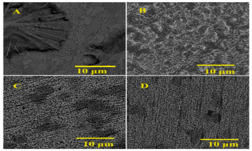
- Excellent etching morphology maintains high-quality results, even under challenging conditions like high copper ion concentrations.
Challenges and Limitations
Despite its numerous benefits, Cu-Mo/Cu-Ti Etching Solution faces challenges and limitations:
- Process optimization necessitates fine-tuning of parameters and comprehensive understanding of substrate properties to achieve optimal etching conditions.
- Environmental considerations are crucial to minimize impact and ensure compliance with chemical usage and disposal regulations.
- Cost considerations, including initial investment and ongoing maintenance expenses, may pose challenges for some manufacturers.
Comparison with Alternative Etching Solutions
Features: Cu-Mo/Cu-Ti Etching Solution
- Multilayer selectivity: Engineered for precise multilayer selectivity, facilitating targeted removal of specific layers like Cu, Mo, and Ti.
- Flexibility in flexible panel fabrication: Crucial in the fabrication process of flexible panels, meeting the demand for bendable and foldable displays.
- Controlled etching rates: Offers controlled etching rates for uniformity and consistency in layer removal.
- Optimized composition: Formulated with an optimized composition for Cu, Mo, and Ti materials, maximizing performance.
- Buffered pH stability: Incorporates a buffering system to maintain stable pH levels, ensuring control and reproducibility throughout the etching process.
Future Developments and Research Directions
Current Trends in Etching Solutions for ICs
Advancements in semiconductor technology are propelling the evolution of etching solutions for ICs. Key trends include promoting environmentally friendly processes and integrating new materials to improve precision. And exploring cutting-edge technologies such as atomic layer etching (ALE) and plasma-assisted etching.
Potential Advancements in Cu-Mo/Cu-Ti Etching Technology
Exciting prospects lie ahead in Cu-Mo/Cu-Ti etching technology. Innovations may focus on enhancing selectivity and efficiency, fine-tuning process parameters for better control, and introducing new formulations to broaden material compatibility. Additionally, efforts may aim at streamlining production processes and cost reduction to widen the applicability of Cu-Mo/Cu-Ti etching solutions.
Areas for Further Research and Improvement
Continued R&D efforts are essential to overcome challenges associated with Cu-Mo/Cu-Ti etching solutions. Key areas for exploration include:
- Understanding etching mechanisms for optimization.
- Exploring sustainable raw material sources.
- Advancing characterization techniques.
- Adapting to emerging semiconductor materials.
- Innovating process integration for seamless workflows.
Environmental and Safety Considerations
Environmental Impact Assessment
Assessing the environmental footprint of Cu-Mo/Cu-Ti etching solutions involves analyzing chemical usage, waste generation, and energy consumption. Utilizing life cycle assessments can guide the development of more eco-friendly processes.
Safety Protocols for Handling Cu-Mo/Cu-Ti Etching Solution
Implementing robust safety protocols is crucial to safeguard workers and the environment. This includes providing appropriate PPE, training on safe handling practices, and establishing emergency response procedures to mitigate risks effectively.
Compliance with Regulations and Standards
Adhering to regulations such as REACH and OSHA guidelines is essential to ensure workplace safety and environmental protection. Regular monitoring and audits help maintain compliance and identify areas for continual improvement in semiconductor manufacturing practices.
In Sum
Cu-Mo/Cu-Ti etching solutions represent a major advancement in integrated circuits. Provides the precise, efficient etching capabilities necessary for the development of modern electronic devices. This solution is capable of selectively removing specific layers while preserving others. This enhances the manufacturing process of high-generation display panels and complex semiconductor substrates. Going forward, continued refinement and research into Cu-Mo/Cu-Ti etching technology is expected to lead to further innovations. Thereby potentially expanding its application and effectiveness across the semiconductor industry. This evolution will play a crucial role in meeting the increasing demands for miniaturization and performance in electronic components.
Access Our Product Catalog and More to Discover High-Performance Chemicals Tailored to Your Business Needs
RECENT ARTICLES
-
 Innovative Oil-Fat Anti-crystallization Solution From UniVOOK Industry!
 -
Concentrated Lysolecithin Powder M-max: Providing Bio-source Active Substance Solutions for the Cosmetics Industry
-
The Solution of Organic Trace Mineral Nutrition Enhancement: Orgamine Cr Tri-Chelated Trace Mineral (Chromium Methionine)

有限公司-scaled.jpg)
有限公司.jpg)