Advanced Metal Etching Solution for Panels: Mo/Al/Mo Formula
Metal etching plays a pivotal role in the manufacturing of semiconductor and display panels, where precision and intricacy are paramount. The Mo/Al/Mo Etching Solution, specifically designed for molybdenum and aluminum layers in these applications, exemplifies the sophistication needed in modern production processes. This formula is crucial not only for the fabrication of integrated circuits (ICs) and generation 8 and above display panels but also in the development of flexible panels. The advancement of metal etching solutions like the Mo/Al/Mo Etching Solution underscores their significance in enhancing the efficiency and capabilities of panel manufacturing, paving the way for more innovative and high-performance electronic devices.
Understanding the Mo/Al/Mo Formula
Composition and Properties of Molybdenum (Mo)
Molybdenum is a transition metal celebrated for its high melting point and superb thermal conductivity, making it indispensable in semiconductor manufacturing. Its robust nature and stability under extreme temperatures are crucial for its role in thin film transistors and integrated circuits. Molybdenum’s excellent electrical conductivity and corrosion resistance make it ideal for complex electronic applications.
Composition and Properties of Aluminum (Al)
Aluminum is highly regarded in the electronics industry for its lightweight, excellent conductivity, and versatility. It is a key component in electronic display production, serving as a conductive layer that significantly enhances image brightness and quality. Aluminum’s ease of processing and superior electrical properties make it a perfect complement to the sturdy molybdenum.
Synergy and Advantages of Combining Mo and Al in the Formula
The strategic combination of molybdenum and aluminum in the Mo/Al/Mo formula offers a dual benefit of strength and conductivity, crucial for precision metal etching. This synergy is key to etching ultra-fine lines necessary for advanced circuit designs and display technologies. The formula supports the production of high-density, high-resolution displays crucial for Generation 8 and above technologies, and enables the development of innovative flexible display technologies for bendable and foldable screens.
Scientific Basis for the Effectiveness of Mo/Al/Mo Formula in Metal Etching
The Mo/Al/Mo formula’s effectiveness in metal etching stems from its capability for selective etching, which accurately targets and dissolves specific metal layers without harming adjacent materials. This selective removal is vital for the detailed layering required in contemporary electronics, facilitating the high precision needed in microelectronics and advanced display manufacturing.
Development Process
Research and Experimentation Phase
Identification of Optimal Ratios of Mo and Al: Initial research focuses on finding the perfect balance of molybdenum and aluminum to optimize conductivity and structural integrity.
Testing Various Chemical Compositions: A range of chemical mixtures is tested to identify the most effective etching solution that works efficiently across different metal layers used in semiconductors and display panels.
Formulation Refinement
Refining the Etching Solution for Maximum Efficiency: Modifications are made to improve the etching speed and effectiveness of the solution, ensuring it meets the demands of large-scale manufacturing.
Stability and Shelf-Life Considerations: The solution is optimized for stability to maintain its effectiveness over time, which is essential for consistent production quality.
Pilot Testing and Validation
Testing the Mo/Al/Mo Formula on Different Metal Panels: The refined formula undergoes testing on various panel types to confirm its versatility and refine its performance across different substrates.
Evaluation of Etching Quality, Speed, and Precision: The final phase of development assesses the etching quality, precision of the etched patterns, and the speed of the process, ensuring compliance with the high standards required for top-tier semiconductor and display production.
Key Benefits of the Mo/Al/Mo Formula
Enhanced Etching Performance
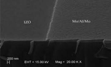
The Mo/Al/Mo Etching Solution is specially designed for the etching of integrated circuits and high-generation display panels, including those for Generation 8 and above. It offers fast etching speeds and minimal side etching, which are crucial for maintaining the integrity of fine patterns on multilayer structures. This solution is characterized by a tapered angle of 45-60 degrees with a Cdloss (single side) of less than 1μm, ensuring sharp and precise patterning without undercut, side engraving, or residue.
Improved Surface Finish and Precision
Thanks to its precise formulation, the Mo/Al/Mo Etching Solution supports high-resolution patterning, essential for the production of large, high-definition displays. It enables fine features to be achieved without damaging underlying or adjacent layers. This contributes significantly to the superior surface finish and detail accuracy required for complex display technology and flexible panel manufacturing.
Reduced Environmental Impact
Unlike traditional etching solutions, Mo/Al/Mo etching solutions do not contain fluoride ions or ferric chloride. Making it a more environmentally friendly option. The reduction of harmful chemicals not only helps minimize environmental impact, but also reduces health risks associated with the manufacturing process. Helps create a safer workplace and reduces chemical waste.
Cost-Effectiveness and Scalability in Production
The Mo/Al/Mo Etching Solution is not only effective but also economical. Its long service life and stability contribute to lower operational costs by reducing the frequency of solution replacement. Additionally, the solution’s formulation is optimized for consistency and controlled etching rates, which are critical for high-volume production settings. This scalability and cost-effectiveness make it an ideal choice for manufacturers looking to expand their production capabilities while maintaining high standards of quality and efficiency.
Applications and Industries
Electronics and Semiconductor Manufacturing
The Mo/Al/Mo Etching Solution is integral in producing integrated circuits and advanced display panels, including Generation 8 and higher, as well as flexible panels. Its ability to etch with high precision is crucial for crafting high-density, high-resolution electronic components essential in the rapidly advancing electronics sector.
Automotive and Aerospace Industries
In the realms of automotive and aerospace, the Mo/Al/Mo Etching Solution is employed to produce durable, lightweight metal components. These industries benefit greatly from the accuracy and reliability of this solution. Ensure components can withstand the rigorous conditions typical of aerospace and automotive environments.
Renewable Energy Sector
The renewable energy sector, particularly in solar and wind power, relies on the Mo/Al/Mo Etching Solution to manufacture components demanding high conductivity and corrosion resistance. The precise etching capability of the solution enhances the efficiency and durability of energy generation and storage devices.
Architectural and Decorative Panel Fabrication
For architectural and decorative panels, Mo/Al/Mo etching solutions can finely etch complex designs onto metal surfaces. Thereby enhancing aesthetic and functional qualities.This application is crucial for producing visually striking and enduring decorative elements for buildings and public spaces.
Future Directions and Innovations
Potential for Further Optimization of the Mo/Al/Mo Formula
Ongoing research could further enhance the Mo/Al/Mo formula, potentially improving the etching speed and precision. These advances could expand its use in existing markets. And helps reduce production costs, making the process more efficient and easy to use.
Integration with Advanced Manufacturing Technologies such as Additive Manufacturing
Integrating the Mo/Al/Mo Etching Solution with state-of-the-art technologies like additive manufacturing (3D printing) opens up new possibilities. This could lead to innovative ways to create complex multilayer materials with unique properties. This expands product functionality and design versatility.
Exploration of New Applications and Markets
The exploration of new applications and markets represents a significant future direction for the Mo/Al/Mo Etching Solution. Opportunities in biotechnology, nanotechnology, and advanced materials research are particularly promising, where precise etching is essential for groundbreaking developments. Expanding into these fields could dramatically extend the solution’s impact and reach.
Closing Thoughts
Mo/Al/Mo The key step in the metal carving area is representative of the wood carving solution. Specially for the production of electronic display panels. Accurate carving ability. The production of modern electric, automobile, and aviation renewable energy sources is a must for high-density, high-separation rate facilities. Moreover, its environmental benefits and potential for integration with cutting-edge technologies like additive manufacturing highlight its future potential. As the industry continues to evolve, Mo/Al/Mo formulations are ready to meet these growing needs. Delivering efficiency and innovation to metal etching processes, setting new standards in manufacturing.
Access Our Product Catalog and More to Discover High-Performance Chemicals Tailored to Your Business Needs
RECENT ARTICLES
-
 Innovative Oil-Fat Anti-crystallization Solution From UniVOOK Industry!
 -
 Concentrated Lysolecithin Powder M-max: Providing Bio-source Active Substance Solutions for the Cosmetics Industry
 -
The Solution of Organic Trace Mineral Nutrition Enhancement: Orgamine Cr Tri-Chelated Trace Mineral (Chromium Methionine)
有限公司-scaled.jpg)
有限公司.jpg)